Difficulty
Difficult
Steps
9
Time Required
- SatNOGS PCB Etching Tutorial 9 steps

User-Contributed Guide
This guide is not managed by the site's staff.
Quiz
0
Introduction
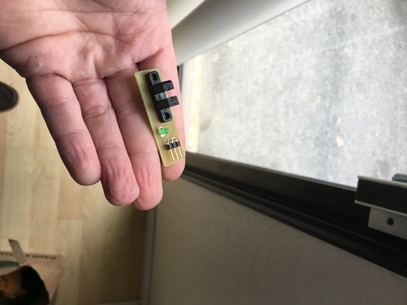
A quick tutorial to show how to create a PCB Board specific to SatNOGS
-
-
Make sure to have all materials which include:
-
Electric Iron
-
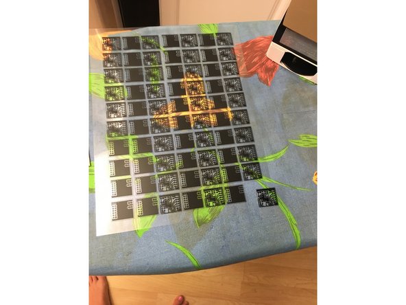
PCB Layout on Over Head Projector Sheet (OHP Sheet) or wax paper
-
Steel Wool
-
Drill
-
Liquid tin
-
Pliers
-
Ferric Chloride
-
-
-
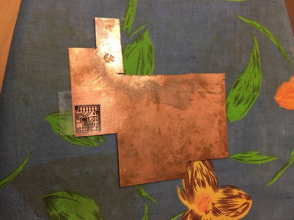
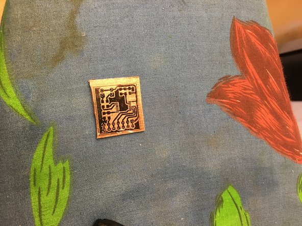
Prepare your copper for PCB process
-
Rub the copper side of the PCB with steel wool. This will remove the top oxide layer of copper and the photo resists layer if any.
-
-
-
Cut out the image of the PCB Layout
-
Make sure the printed/mirror side should be placed on the copper side of the PCB.
-
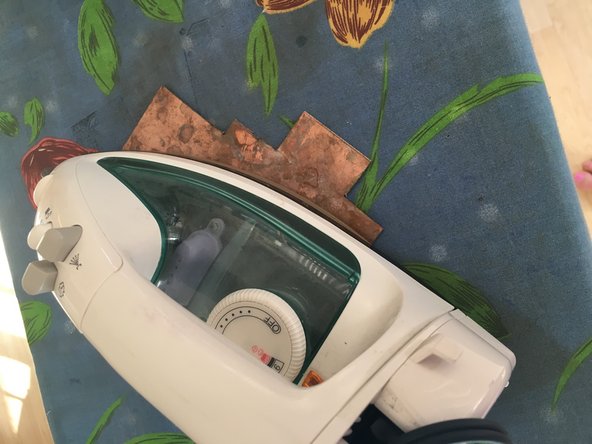
Transfer the image using an electric iron
-
-
-
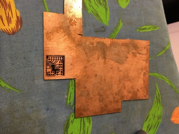
Let the PCB plate cool down before removing the OHP sheet.
-
Because this is a manual process, be aware that the layout does not always properly come off. (Sometimes the tracks are broken in-between)
-
Use a permanent market to complete the tracks properly
-
Cut out the PCB plate, and drill the holes.
-
-
-
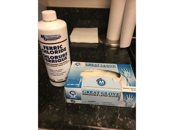
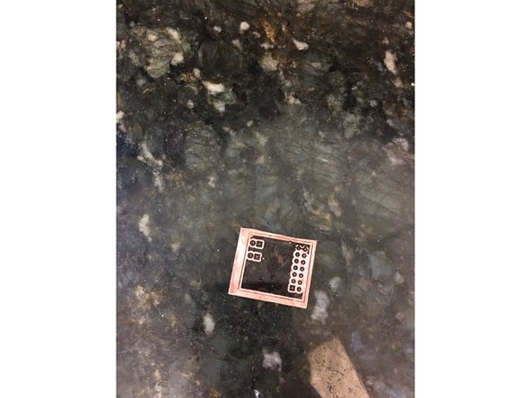
The unmasked area is the unwanted copper that is not covered by ink.
-
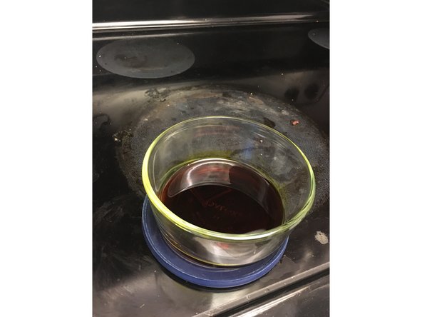
To remove this, submerge the PCB in Ferric Chloride
-
Make sure to cover the back side of the PCB in order to prevent it from being corroded. This can be done using tape or by covering it with sharpie ink.
-
Dip the PCB in the etching solution for about 30 minutes.
-
-
-
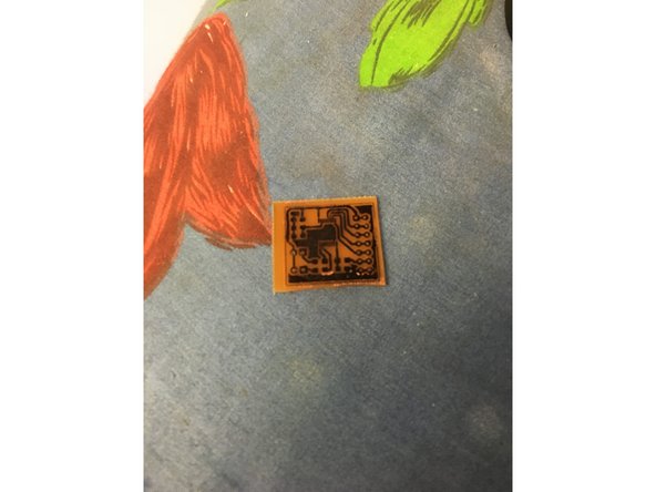
Use pliers to take out the PCB, and check to make sure the entire unmasked area has been etched.
-
-
-
Align the other side of the design with the holes in the copper board.
-
Repeat Steps 5 and 6.
-
-
-
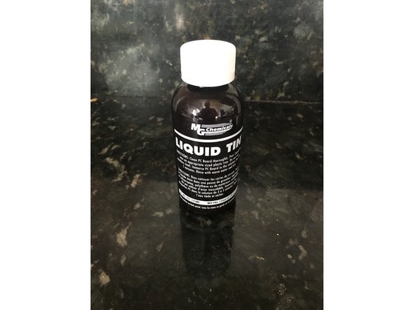
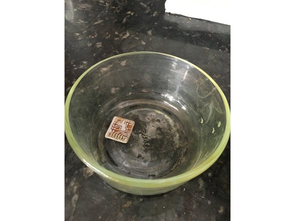
Tinning is not required but is used to improve the qualities
-
Place the PCB immersed in the liquid tin for about only a minute before removing it
-
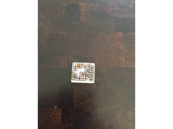
Finalize the board by removing the excess copper on the edges (if any).
-